PVD Copper Coating on Glass Substrates
As the semiconductor industry evolves, Glass Core Substrates have become a core material platform for 2.5D/3D advanced packaging, CPO (co-packaged optics), and high-frequency RF devices. However, there is a major physical challenge: copper has inherently poor adhesion to glass.
We use advanced PVD (physical vapor deposition) magnetron sputtering technology to successfully solve the copper adhesion challenge on glass substrates.
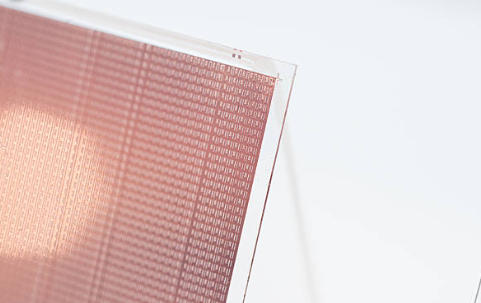
Our core PVD copper coating capabilities:
- Through our proprietary semiconductor coating technology, we have developed two unique processes: precision PVD sputtering coating and high-adhesion coating.
- PVD copper thickness can reach up to 10 µm.
- For ultra-thin glass after copper coating, we can solve the problem of residual stress inside the metal thin film, which causes severe warpage or even breakage of ultra-thin glass (such as 0.05T TFT glass).
- Whether for small-size glass wafers or large-size glass panels, our magnetron sputtering can achieve uniform copper film thickness.
- After our PVD coating, the film layer features strong stability, high hardness, high wear resistance, high corrosion resistance, strong chemical stability, and long film life. The coating process is non-toxic and does not generate pollutants.
PI slurry synthesis for coating and curing to protect the copper circuits
After PVD copper coating, we use in-house PI slurry synthesis for coating and curing to protect the copper circuits, providing insulation, stress control, and prevention of signal crosstalk. We use high-precision spin coating technology to achieve precise control of the PI film layer.
- PI is currently the most heat-resistant polymer material that can be practically applied, while also maintaining good performance at low temperatures. It remains stable without deformation over the long term in the range of -269°C to 280°C.
- PI material demonstrates excellent performance in processability, mechanical properties, insulation, flame retardancy, chemical corrosion resistance, radiation resistance, and many other aspects.
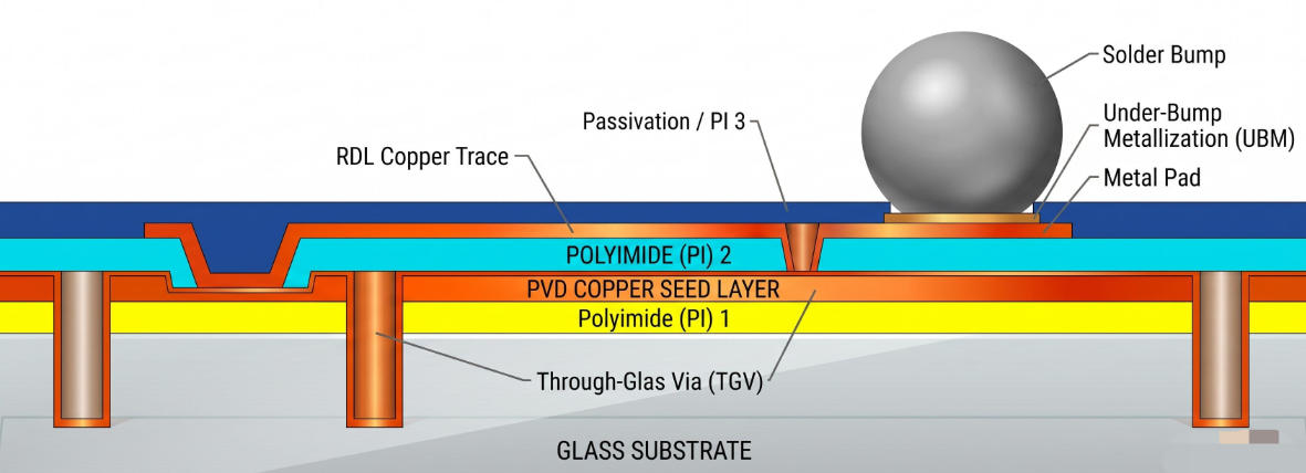
Our one-stop service of PVD copper-coated glass substrates + PI passivation currently serves the following R&D and mass-production projects
It including:
- TGV glass through-via carrier substrates: providing a reliable RDL base for multi-chip integration
- Semiconductor glass substrates
- CPO co-packaged optics and optical communications: providing flat, highly insulating, high-dielectric-strength precision circuits
- Mini/Micro LED packaging substrates
- Glass microfluidic chips: integrating stable electrodes and microheaters on biochips
If you are looking for glass substrates that shorten the supplier chain and improve project yield, contact our engineering team to discuss customized “Glass Substrate PVD + PI” process solutions that meet your project metrics.