TGV (Through-Glass Via) Technology
Through-Glass Via (TGV) technology has become a focal point in advanced semiconductor packaging, glass-core substrates, and co-packaged optics. Leveraging our extensive expertise in micro/nano-manufacturing and ultra-precision laser processing, we have established a globally competitive system for both the R&D and mass production of TGV solutions.
We possess full-chain capabilities, spanning glass thinning, cutting, and laser-based TGV (Through-Glass Via) drilling, through to PVD copper metallization, PI (polyimide) passivation, and final inspection and delivery. We offer a comprehensive, one-stop solution—integrating glass processing, TGV, PVD copper metallization, and PI passivation—that supports prototyping, validation, and mass-production implementation for applications such as TGV glass interposers, glass core substrates, CPO/RF substrates, glass-based microfluidics, and Mini/Micro LED packaging substrates
Core Technical Advantages of TGV
By integrating advanced, ultra-high-speed laser technology with optimized process workflows, our TGV solutions achieve industry-leading performance in terms of production efficiency, processing precision, and product yield.
- Utilizing high-energy micro/nano-laser processes, we can achieve via diameters as small as 3μm and aspect ratios as high as 150:1, effectively meeting the requirements for high-density interconnects.
- We possess high-throughput via-forming capabilities, with processing speeds reaching 5,000 vias per second, and support the flexible creation of both blind and through-vias.
- Glass substrates inherently offer excellent physical properties; our processes ensure the mechanical stability of these substrates while effectively minimizing and controlling potential warpage.
- We are currently capable of processing large-format substrates (up to 650mm × 650mm) with thicknesses as low as 0.05mm, providing a robust solution for large-scale commercial mass production.
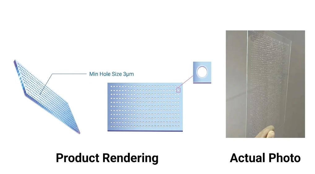
TGV Through Glass Via Technical Capability Datasheet
Our Core Offering: Through-Glass Via (TGV) Solutions
- TGV Substrates
- Glass-Core Substrates
- Substrates for Co-Packaged Optics (CPO) and High-Frequency RF Applications
- Glass-Based Microfluidic Devices
- Substrates for Mini/Micro LED Packaging and Micro LED Glass Substrates
We prioritize “verifiable manufacturing capabilities”:
Quality inspection is integrated into every stage—thinning, dicing, via formation, copper metallization, and passivation.
MES (Manufacturing Execution System) integration ensures full transparency of production data.
On-time delivery rate ≥99%; process yield ≥99%.
In-house logistics fleet providing direct, point-to-point service to our clients.
Comprehensive engineering support—from process evaluation and prototyping to small-batch validation—for projects involving ultra-thin glass, TGV, Glass-Core Substrates (GCS), CPO/RF, and microfluidics.
If you are seeking a TGV glass substrate manufacturing partner to streamline your supply chain and improve project yields, we offer customized process solutions—combining precision glass machining, TGV formation, PVD copper metallization, and polyimide (PI) passivation—tailored to your specific project requirements. Contact us to discuss a one-stop TGV and metallization solution designed to meet your project’s technical specifications.