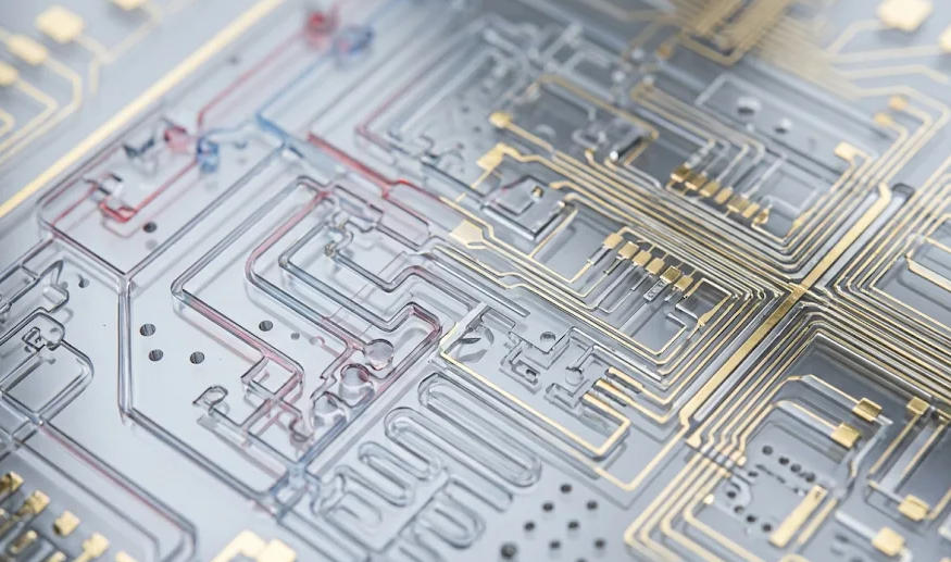
Microfluidic MEMS Glass Substrates
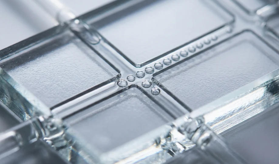
We manufacture glass substrates for microfluidic MEMS devices, offering options such as borosilicate glass 3.3 and quartz/fused silica. Customization is supported for microchannels, cavities, reservoirs, TGV glass vias, inlets/outlets, alignment marks, bonding areas, and optical windows. We can combine wet etching, laser cutting, CNC machining, drilling, glass-to-glass thermal bonding, glass-to-silicon anode bonding, and metallization processes, covering everything from prototype prototyping to mass production.
MEMS Glass Substrates, Glass Microfluidic Substrates, Glass Through-Hole TGV, Glass Anodic Bonding, Microchannel Etching, ,
Microfluidic MEMS Glass Substrates Product Discription
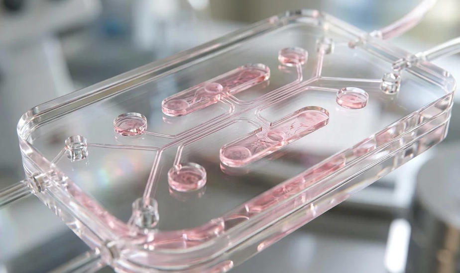
Microfluidic MEMS glass substrates serve as essential base materials or cover plates for MEMS microfluidic devices, such as micropumps, microvalves, flow/pressure sensors, micro-nozzles, lab-on-a-chip systems, and microreactors. These glass substrates are typically used to form microchannels, cavities, through-glass vias (TGVs), optical windows, insulating layers, and bonding interfaces, and are integrated with silicon, other glass types, or various additional materials. They are commonly employed in applications including MEMS flow sensors, biosensors, and microfluidic sensors for liquids and gases.
Coligh provides custom-fabricated microfluidic MEMS glass substrates based on client drawings. These can incorporate features such as microchannels, reaction/back-pressure cavities, through-glass vias (TGVs), fluid inlet/outlet ports, alignment marks, bonding zones, optical windows, and metallized regions.
Our current material offerings include borosilicate glass 3.3, quartz, and fused silica. We utilize a range of processes—including wet etching, laser cutting, CNC machining, laser drilling, glass-to-glass thermal bonding, glass-to-silicon anodic bonding, and metallization—to meet specific design requirements.
Microfluidic MEMS Glass Substrates Product Features:
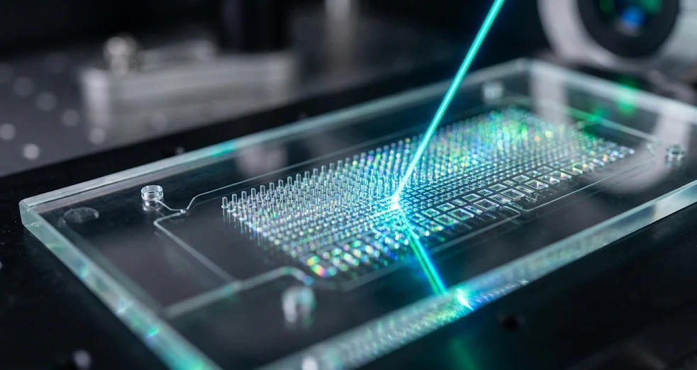
- Borosilicate glass and quartz/fused silica offer excellent optical transparency, with surface flatness, roughness, and cleanliness levels that can be controlled to meet the stringent requirements for optical windows.
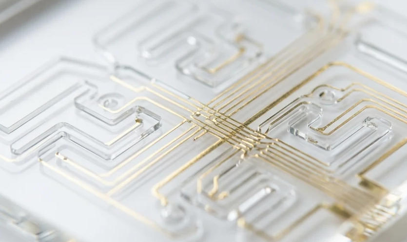
- Glass possesses superior electrical insulation properties, making it suitable for use as an electrode isolation layer, an insulating substrate, or an electrically isolated region. It can be metallized to form electrode patterns, or left as bare glass to provide electrical isolation.
- We specialize in the fabrication of microchannels, reaction/back-pressure chambers, fluid reservoirs, nozzle micro-orifices, and optical windows on substrates such as borosilicate glass 3.3 and quartz/fused silica. By combining processes—including wet etching, laser cutting, CNC machining, and drilling—we can create complex single-layer or multi-layer microstructures based on your technical drawings.
- Leveraging laser/ultrasonic drilling, etching, and CNC machining, we evaluate the manufacturability of Through-Glass Vias (TGV), fluid inlet/outlet ports, alignment marks, and bonding zones, ensuring precise positional accuracy, hole diameters, and aspect ratios.
- We offer glass-to-glass thermal bonding, enabling the sealing of etched microchannels, cavities, and through-holes to form airtight fluidic pathways or enclosed chambers.
We can also evaluate glass-to-silicon anodic bonding solutions, providing custom fabrication of cavities, through-holes, bonding zones, and alignment marks on borosilicate glass cover plates or substrates.
Why Choose Our Microfluidic MEMS Glass Substrates For MEMS
- Glass possesses a high dielectric constant and excellent electrical insulation properties, making it highly suitable for bio-electrical sensing. Furthermore, glass offers high optical transparency; for instance, borosilicate glass features a coefficient of thermal expansion (CTE) that enables stress-free bonding with silicon.
- Our etching processes—including deep reactive ion etching (DRIE) and wet etching—achieve extremely high aspect ratios and superior sidewall verticality. These techniques allow for the creation of through-glass vias (TGVs) that serve as fluidic inlets and outlets.
- We offer both anodic bonding (glass-to-silicon) and direct bonding (glass-to-glass) at the wafer level, meeting the stringent bonding requirements for MEMS devices.
- For microfluidic MEMS glass substrates, we provide agile foundry services—supporting everything from initial prototyping to wafer-level mass production—to help customers accelerate their time-to-market.
- Our expertise in glass micromachining is backed by proprietary processes for managing glass brittleness, controlling internal stress, and executing laser-induced modification for TGV (through-glass via) fabrication.
Our Custom Capability Of MEMS Micropump Glass Substrates
| Customization Item | Capabilities |
|---|---|
| Glass Material | Borosilicate Glass 3.3, Quartz Glass / Fused Silica, Soda-Lime Glass |
| Substrate Dimensions | Customized according to product drawings, up to 650 × 650 mm |
| Glass Thickness | 0.05–2 mm |
| Microstructure Fabrication | Microgrooves, microcavities, microhole arrays, microsteps, microprotrusions, etc. |
| Microchannel Fabrication | Straight channels, serpentine channels, branching channels, cross channels, complex channel structures, etc. |
| Microchannel Width | ≥ 10 μm |
| Microchannel Depth | ≥ 3 μm |
| Microhole / Through-Hole Fabrication | Through-holes, blind holes, inlet ports, outlet ports, alignment holes, mounting holes, etc. |
| Microhole Diameter | ≥ 3 μm |
| Microchamber Fabrication | Reaction chambers, detection chambers, pressure chambers, fluid chambers, vacuum chambers, etc. |
| Multi-Layer Structures | Multi-layer glass structures, stacked microchannels, integrated complex microstructures |
| Metallization | Cr, Au, Ti, Pt, ITO thin films and conductive layers |
| Bonding Processes | Glass-to-Glass Bonding, Glass-to-Silicon Bonding, Anodic Bonding, Thermal Bonding, Adhesive Bonding |
Microfluidic Sensor Glass Substrates Applications
Glass Substrates for Microfluidic MEMS Devices
Microfluidic MEMS devices typically require microchannels, cavities, through-holes, optical windows, and reliable bonding interfaces, while also demanding substrates that are chemically inert, electrically insulating, and dimensionally stable. With its high rigidity, transparency, chemical inertness, and electrical insulation, glass is well-suited for use as a substrate or cover plate for MEMS microfluidic devices, as it can be micro-machined and bonded to silicon or other glass components.
Glass Substrates for MEMS Pressure Sensors
MEMS pressure sensors require stable cavities, robust bonding interfaces, electrically insulating substrates, and reliable sealing. Glass is chemically inert and electrically insulating; it can be machined to include cavities and through-holes, making it an ideal substrate or cover plate for pressure sensors. Borosilicate glass, in particular, offers a thermal expansion coefficient well-matched to that of silicon, facilitating glass-to-silicon anodic bonding.
Glass Substrates for Microfluidic Control Chips
Microfluidic control chips—which handle functions such as flow switching, distribution, mixing, and flow-rate regulation—require consistent channel dimensions, secure bonding/sealing, chemical inertness, and electrical insulation. Thanks to its high rigidity, resistance to channel deformation, and compatibility with a wide range of reagents, glass is well-suited for precision flow control and the creation of electrically isolated structures.
Glass Substrates for Micropumps and Microvalves
Micropumps and microvalves require stable pump or valve cavities, microchannels, reliable bonding, and consistent dimensions. Glass offers the necessary rigidity, chemical inertness, and electrical insulation to form these cavities, flow paths, and bonding interfaces. Techniques such as glass-to-glass or glass-to-silicon anodic bonding can be used to create robust, sealed structures.
Glass Substrates for Microreactors
Microreactors require resistance to chemical solvents, low adsorption, effective mixing structures, and optical windows for observation. Glass is chemically inert, exhibits low leaching, is transparent, and withstands various reagents and cleaning processes, making it ideal for micro-scale mixing, chemical reactions, and in-situ optical monitoring.
Glass Substrates for Microsensors and Detection Chips
Microsensors and detection chips often require optical windows, electrically insulating substrates, stable cavities, and surfaces that can be metallized. Glass is transparent, flat, electrically insulating, and chemically inert, making it well-suited for optical detection, electrode isolation, and the integration of sensing zones.
Glass Substrates for Biomedical MEMS Devices
Biomedical MEMS devices often involve the handling of minute quantities of liquids, contact with reagents, optical detection, and the need for electrical insulation. Due to its chemical inertness, low adsorption, transparency, electrical insulating properties, and ease of cleaning, glass is an ideal material for use as a substrate or cover plate in biomedical MEMS.